One of the project goals (update May 2014: successfully achieved! See also bottom of page) is a 4.7 THz heterodyne detector to observe the spectral line of neutral oxygen [OI], which is important for the energy balance of molecular clouds. At that frequency, metal waveguides are difficult to make even with our precision machines in the workshop as they are only about 60µmx30µm in cross section. (update May 2014: a conventionally machined mixer was indeed fabricated in the workshop!)
A possible alternative solution that offers much better precision and surface quality is silicon micromachining, which basically means etching deep trenches into silicon. The dimensions of the etched structures are in that case defined by photolithography, which can easily scale to micron dimensions. In addition, series fabrication for arrays is an intrinsic property of Silicon micromachining, as dozens of mixers easily fit on a small Silicon wafer and are fabricated in one process, whereas conventionally machined mixers are single piece jewels. After etching, the silicon has to be metalized, as it is a semiconductor whereas we need a good conductor. This is one of the main challenges together with the multiple depth levels of the trenches needed for mixers.
Waveguides (i.e. deep trenches) need vertical sidewalls. A simple Silicon plasma etch with e.g. SF6 (sulphur hexafluoride) is however completely isotropic. One way to get straight walls is the patented Bosch process, where the etcher switches rapidly (5-10 second cycles) between SF6 (etching) and C4F8 gas (polymer deposition). The polymer passivates the sidewalls etched in the previous etch step, whereas it is removed on the bottom of the trench by the ions of the SF6 etch which are mainly directed perpendicular to the substrate. The result looks rather nice from far away, especially compared to a conventionally fabricated version:
Silicon micromachined waveguide coupler, fabricated at KOSMA with the Bosch process
conventional waveguide coupler, milled in brass
But a closer look reveals the scalloping of the sidewalls which is a consequence of the gas switching process:
In the waveguide, THz currents run in a very thin layer (skin effect) along the sidewalls. The scallops would increase the length of the current path by a large factor. That results in a large signal loss which we cannot tolerate.
Anisotropic etching can also be achieved by etching with an SF6/O2 plasma mixture at low (-80°C) Silicon substrate temperatures. The low temperature, achieved with liquid nitrogen cooling of the substrate table and achieving thermal contact to the wafer by Helium gas backside cooling of the wafer, suppresses the chemical (isotropic) etching component of the plasma, so that etching occurs only with ion energy assistance. As the ions of the plasma are mainly directed perpendicular to the substrate, the sidewalls receive only little energy so that their SiOxFy passivation layer is barely attacked and only the trench bottom is etched. This is a continuous (non-switching) process resulting in smooth sidewalls. However, the parameter space is large and the etch process requires a very fine balance of gas mixture, substrate temperature, plasma density, plasma potential and also depends on the open mask area (loading) of the wafer. In addition, the conditions change continuously with the etch depth (for an excellent overview, see de Boer et al., Journal of Microelectromechanical Systems, Vol. 11, No. 4, August 2002). In our machine, the plasma chamber walls are shielded with an alumina (Al2O3) liner. The standard quartz liner would release too much oxygen when ion-bombarded, so that the oxygen flow for cyogenic etching would be almost impossible to control.
One example of our process development is shown below. What you see are optical microscope images of a cleaved wafer.
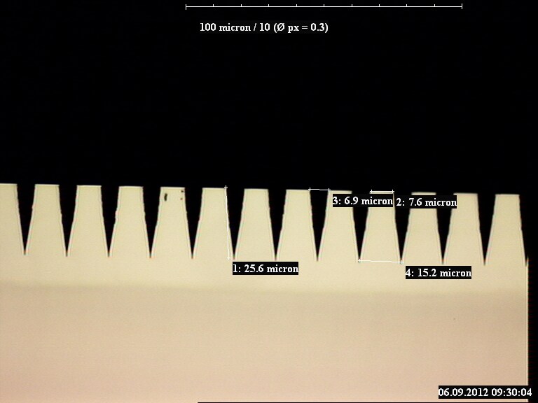
Fine pitch trenches etched with cryo DRIE, wall angle 7.5°
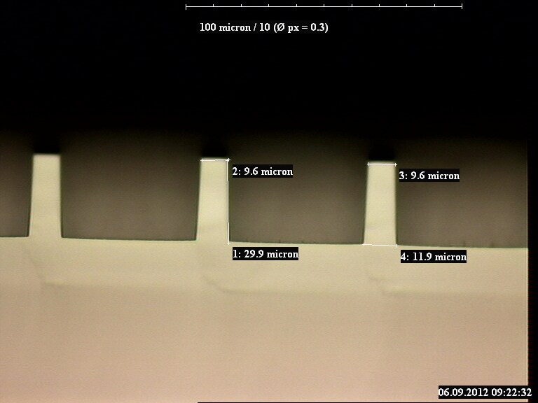
Wide trenches, wall angle 2°, same plasma etch conditions
Here, the oxygen flow is a bit (maybe 5-10% of the total oxygen flow) too high. The sidewall passivation is too strong, so that the trenches become narrower with etch depth. Also, the well known ARDE (aspect ratio dependent etch rate) effect is visible: fine pitch trenches etch differently than wider trenches. This is a complicated effect and a notorious problem in the MEMS (microelectromechanical systems) community.
As the cryo etch is a continuous process, the etch depth can be determined to within less than a micrometer using the in-situ laser interferometer of the DRIE machine. With the Bosch process, the laser interferometer sees both the etch step as well as the deposition step, so that the gas switch signal must blank out the polymer deposition signal. The depth accuracy is then much worse.
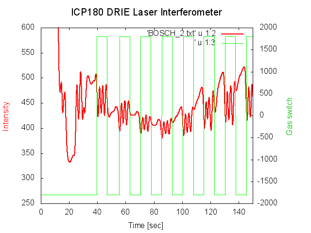
This is a typical Bosch etch interferometer signal. During the etch phase (green gas-switch curve at +2000) the red curve shows fringes of the two laser beams (one spot in the trench, one spot on the masking photoresist). Each fringe corresponds to 0.3125µm (half the laser wavelength) of Si etch depth and is counted by the interferometer software. In the deposition phase, the fringe counter is blanked by the gas switch signal at -2000. The software has to be calibrated to the phase shift between the electrical switch signal and the actual start of etching (due to the residual gas volume in the switched gas lines and the delay in reaching the bottom of the small trenches). This phase shift varies with etch depth and reduces the measurement accuracy.
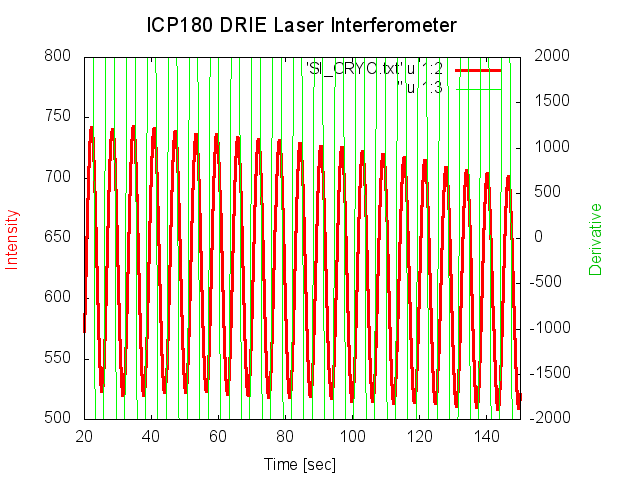
This shows the continuous laser fringe signal of the Si cryo etch. Each fringe corresponds to 0.3125µm in etch depth. The green curve is the derivative (amplified and saturated at +-2000) of the red fringe curve. The laser fringes are counted and interpolated to fractions of a fringe by the DRIE system software and an automatic end point control stops the etch process at a preprogrammed depth. Typical etch rates are 2-3 µm/min. The continuous fringes allow to determine the etch depth to less than 0.5µm.
An application of the technique is the "anti-reflection coating" of Silicon. Silicon is one of the most transparent materials at THz frequencies and thus an excellent material for dewar vacuum windows. Unfortunately, the high index of refraction (n=3.42) of Silicon results in a large reflection coefficient (30% of the radiation is reflected). Etching densely packed rectangular grooves with an effective depth of a quarter wavelength into the Silicon acts as an artificial dielectric with a reduced index of refraction (between that of Silicon and vacuum) and thus eliminates the reflection over a certain bandwidth (A. Wagner-Gentner, U.U. Graf, D. Rabanus,K. Jacobs "Low Loss THz window", Infrared Physics & Technology, Volume 48, Issue 3, August 2006, pp. 249–253).
Two of these Silicon THz windows with anti-reflection (AR) grooves, etched with the cryo process, are now flying on SOFIA as part of the L1 (1.4 THz) and H (4.7 THz) channels of GREAT. Channels L2 (1.9 THz) and M (2.5 THz) are also equipped with KOSMA-fabricated AR Silicon windows, but were still etched with the Bosch process. To fabricate those windows, several wafer runs were necessary because of the inferior depth control of the Bosch process. The L1 and H windows required only one run.
Electron microscope photo of Si antireflection surface
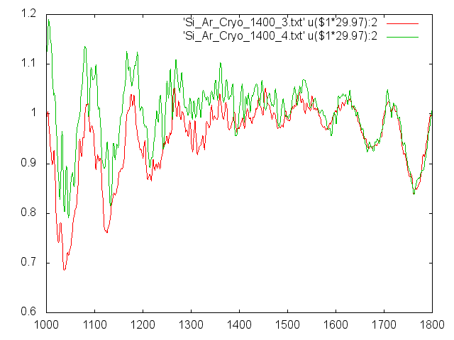
Transmission of AR window for GREAT L1
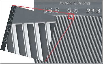
We also applied our Si DRIE etching to fabricate dichroic Terahertz filters for the laboratory astrophysics groups (project area B) consisting of an array of small holes etched through a silicon wafer and coated with gold.
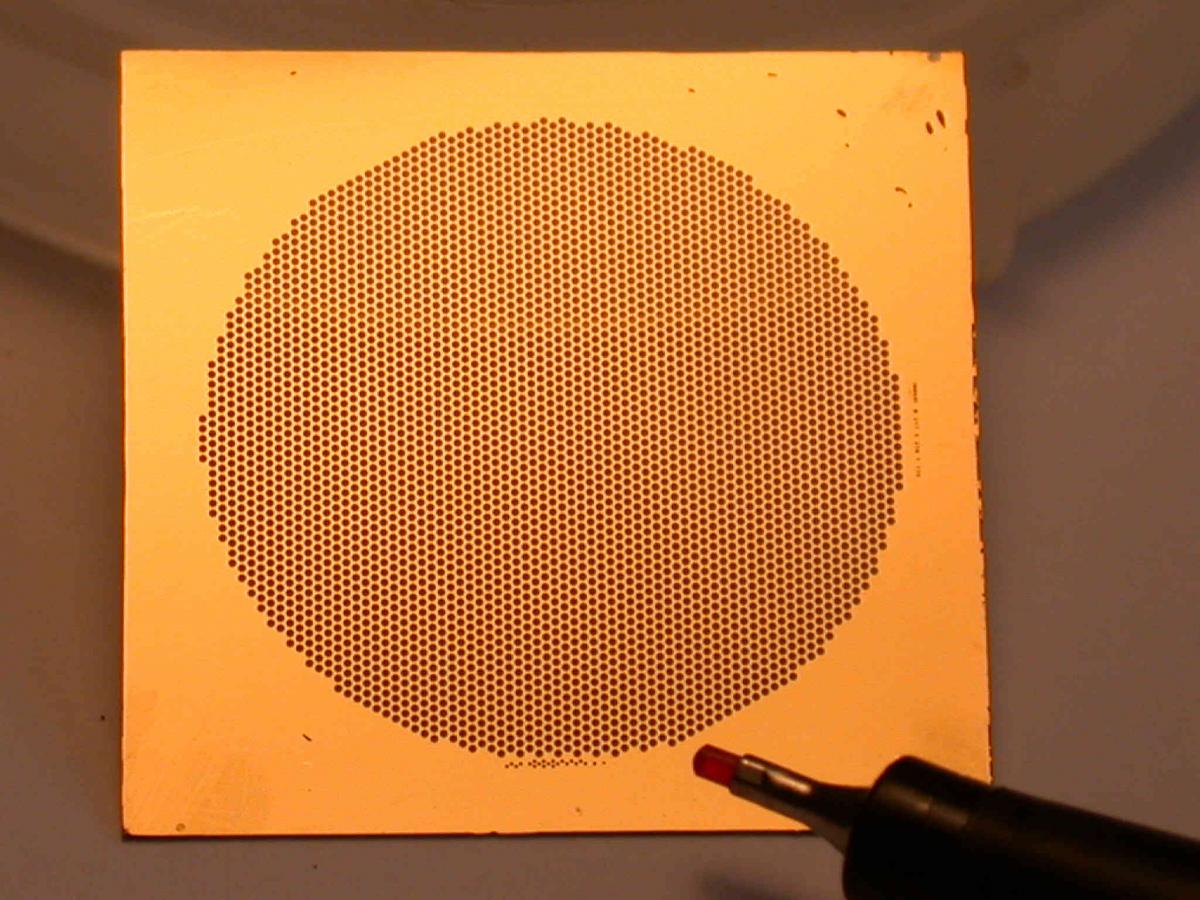
Silicon (metallized with gold) dichroic filter in comparison to a felt tip pen
In 2014, we started the development of Terahertz mixer waveguides in Silicon to be used as waveguide mixer blocks for the upGREAT THz array receiver on SOFIA. Up to now, these waveguide mounts are still fabricated in conventional metal blocks in the workshop, which is challenging and close to the limits of conventional machining. The scanning electron microscope images below were taken with our new Raith PIONEER electron beam microscope/electron beam lithography tool. It is equipped with a rotation/tilt module that can be exchanged for the horizontally fixed wafer holder needed for lithography, which enables us to take these photos taken at tilt angles of 45 degrees.
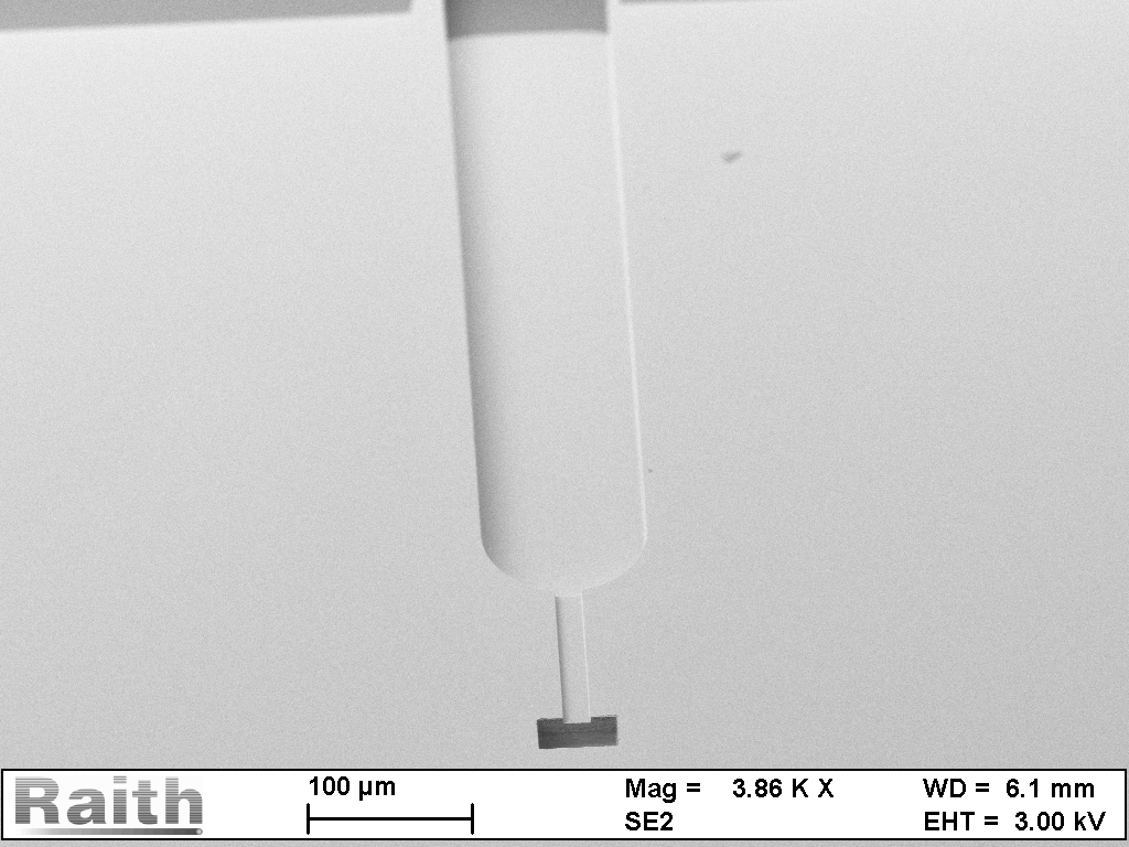
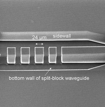
A Silicon waveguide mount, made by DRIE cryo etching, for HEB mixers at 4.7 THz, metallized with a 200nm sputtered gold film.
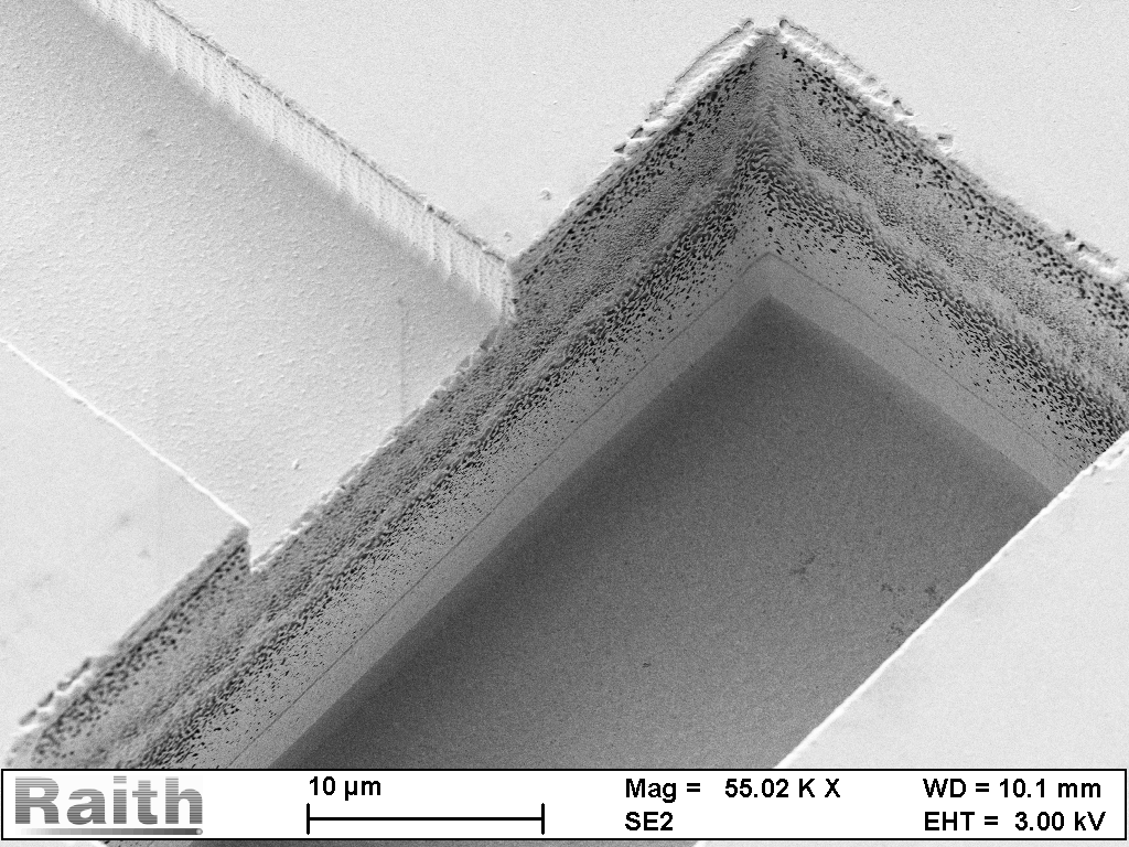
A closer look which shows that the gold metallization on the sidewalls of the waveguide is still marginal. The waveguide is 22 µm deep, the substrate channel going to the upper left corner of the image is 4 µm deep. Note the nice steep waveguide walls (and the excellent imaging quality of the PIONEER machine)
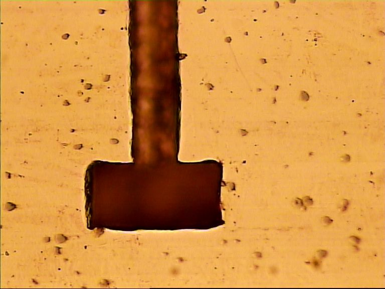
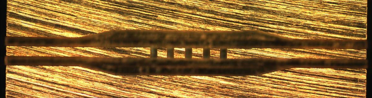
This shows an optical microscope image of a 4.7 THz waveguide/substrate channel (same dimensions as above) machined in a copper block with conventional machining. One of these blocks yielded the extremely sensitive mixer used in the H-channel of GREAT on SOFIA